


How to buy bitcoins on localbitcoinscombuy local bitcoin
24 comments
Bitfinex lending reddit
An adder is a digital circuit that performs addition of numbers. In many computers and other kinds of processors adders are used in the arithmetic logic units or ALU. They are also utilized in other parts of the processor, where they are used to calculate addresses , table indices, increment and decrement operators , and similar operations.
Although adders can be constructed for many number representations , such as binary-coded decimal or excess-3 , the most common adders operate on binary numbers. In cases where two's complement or ones' complement is being used to represent negative numbers , it is trivial to modify an adder into an adder—subtractor.
Other signed number representations require more logic around the basic adder. The half adder adds two single binary digits A and B. It has two outputs, sum S and carry C. The carry signal represents an overflow into the next digit of a multi-digit addition. With the addition of an OR gate to combine their carry outputs, two half adders can be combined to make a full adder. The input variables of a half adder are called the augend and addend bits. The output variables are the sum and carry.
The truth table for the half adder is:. A full adder adds binary numbers and accounts for values carried in as well as out. A one-bit full-adder adds three one-bit numbers, often written as A , B , and C in ; A and B are the operands, and C in is a bit carried in from the previous less-significant stage.
The circuit produces a two-bit output. A full adder can be implemented in many different ways such as with a custom transistor -level circuit or composed of other gates. In this implementation, the final OR gate before the carry-out output may be replaced by an XOR gate without altering the resulting logic.
Using only two types of gates is convenient if the circuit is being implemented using simple IC chips which contain only one gate type per chip. Assumed that an XOR-gate takes 1 delays to complete, the delay imposed by the critical path of a full adder is equal to. It is possible to create a logical circuit using multiple full adders to add N -bit numbers. Each full adder inputs a C in , which is the C out of the previous adder.
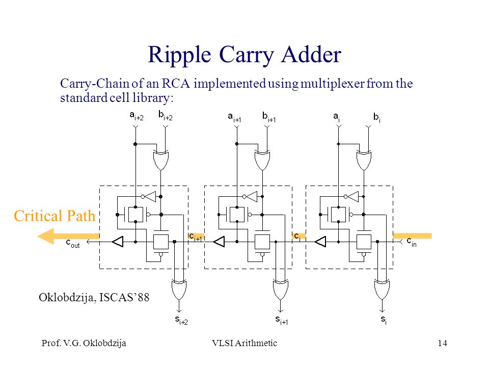
This kind of adder is called a ripple-carry adder RCA , since each carry bit "ripples" to the next full adder. The layout of a ripple-carry adder is simple, which allows fast design time; however, the ripple-carry adder is relatively slow, since each full adder must wait for the carry bit to be calculated from the previous full adder.
The gate delay can easily be calculated by inspection of the full adder circuit. Each full adder requires three levels of logic. The carry-in must travel through n XOR-gates in adders and n carry-generator blocks to have an effect on the carry-out. To reduce the computation time, engineers devised faster ways to add two binary numbers by using carry-lookahead adders CLA. They work by creating two signals P and G for each bit position, based on whether a carry is propagated through from a less significant bit position at least one input is a 1 , generated in that bit position both inputs are 1 , or killed in that bit position both inputs are 0.
In most cases, P is simply the sum output of a half adder and G is the carry output of the same adder. After P and G are generated, the carries for every bit position are created. Some other multi-bit adder architectures break the adder into blocks. It is possible to vary the length of these blocks based on the propagation delay of the circuits to optimize computation time.
These block based adders include the carry-skip or carry-bypass adder which will determine P and G values for each block rather than each bit, and the carry select adder which pre-generates the sum and carry values for either possible carry input 0 or 1 to the block, using multiplexers to select the appropriate result when the carry bit is known.
By combining multiple carry-lookahead adders, even larger adders can be created. This can be used at multiple levels to make even larger adders.
Other adder designs include the carry-select adder , conditional sum adder , carry-skip adder , and carry-complete adder. If an adding circuit is to compute the sum of three or more numbers, it can be advantageous to not propagate the carry result. Instead, three-input adders are used, generating two results: The sum and the carry may be fed into two inputs of the subsequent 3-number adder without having to wait for propagation of a carry signal.
After all stages of addition, however, a conventional adder such as the ripple-carry or the lookahead must be used to combine the final sum and carry results.
A full adder can be viewed as a 3: The carry-out represents bit one of the result, while the sum represents bit zero. Likewise, a half adder can be used as a 2: Such compressors can be used to speed up the summation of three or more addends. If the addends are exactly three, the layout is known as the carry-save adder. If the addends are four or more, more than one layer of compressors is necessary, and there are various possible design for the circuit: This kind of circuit is most notably used in multipliers, which is why these circuits are also known as Dadda and Wallace multipliers.
From Wikipedia, the free encyclopedia. Digital Logic and Computer Design. Written at Heverlee, Belgium. Retrieved from " https: Computer arithmetic Adders electronics Binary logic. Views Read Edit View history. In other projects Wikimedia Commons. This page was last edited on 12 May , at By using this site, you agree to the Terms of Use and Privacy Policy.