Digital Logic Design
4 stars based on
55 reviews
This is an open access article distributed under the Creative Commons Attribution Licensewhich permits unrestricted use, distribution, and reproduction in any medium, provided the original 4 bit ripple adder vhdl code for xnor is properly cited. Addition usually affects the overall performance of digital systems and an arithmetic function.
Adders are most widely used in applications like multipliers, DSP i. In digital adders, the speed of addition is constrained by the time required to propagate a carry through the adder. Various techniques have been proposed to design fast adders. In any processing unit, adders are basic building block. We look for an area and power efficient fast adders to increase system performance [ 12 ].
Ripple carry adders RCA [ 3 ] are area and power efficient, but with drawback of being slow. Carry-select adders CSA [ 24 — 10 ] are one of the fastest adders among traditional adders, but they are not power and area efficient. The organization of this 4 bit ripple adder vhdl code for xnor is as follows. Section 2 deals with the analysis of adder using different topologies. Section 3 presents logic for CBL adder design. Section 4 deals with comparative analysis based on delay, area, and power among different adder architectures using Synopsis Design Compiler.
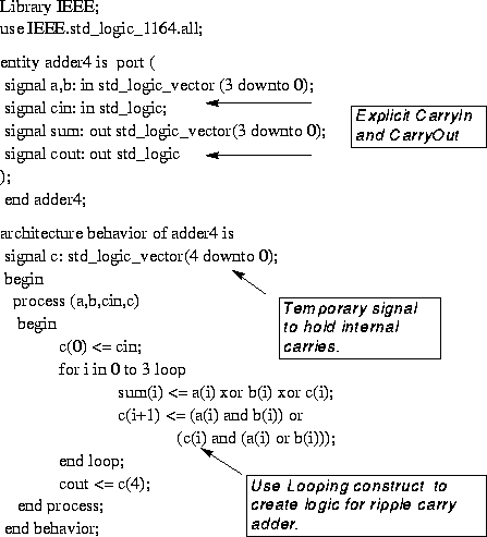
The fault testing concept s-a-0, s-a-1 for various adders is also discussed. Section 5 gives the conclusion followed by the references. It is basic parallel adder where a chain of adders is cascaded with carry rippled from one stage to another. Block diagram for 4-bit RCA is shown in Figure 1 a. Delay is due to the rippling of carry since the consequent blocks of adder have to wait for the carry generated from the previous adder.
A bit RCA is shown 4 bit ripple adder vhdl code for xnor Figure 1 b. There are 16 blocks and each block is a 4-bit RCA. Each block has 4 full adders except the first block which has 3 full adders and 1 half adder as the lowest bit of addends 4 bit ripple adder vhdl code for xnor be added using the half adder instead of a full adder.
CLA use the concept of generating carry and propagating carry. Carry propagates if either of or is 1: On simplifying, we have Expressions shown above are implemented using a two-level AND-OR circuit so that can be evaluated very quickly. Due to independent computation of carry, the CLA based adder is fast as compared to RCA but at a cost of increased hardware. Block diagram for 4-bit CLA is shown in Figure 2 a.
Figure 2 b shows bit adder based on CLA blocks. There are 16 blocks. Each block is of 4 bits and has circuit as shown in Figure 2 a. The carry generated from any block is rippled to its successor block. This is not a pure bit adder. It has been implemented just for 4 bit ripple adder vhdl code for xnor purpose. The carry-select adder consists of two ripple carry adders and a set of multiplexers.
The block diagram for 4-bit addition using CSA is given in Figure 3 a. After the 4 bit ripple adder vhdl code for xnor results are available, the correct sum and carry-out are then decided by the multiplexer once the correct carry is known [ 4 ].
For designing bit adder, we can cascade the structure shown in Figure 3 a. The number of bits in each CSA block is uniform.
Figure 3 b shows block diagram of bit CSA. There are 2 blocks, each having 8 blocks consisting of 4-bit RCA. All blocks other than RCA0 are in pair whose is connected to logic 0 or 1 which acts as and the results of whom block is to be considered depend upon the carry propagating from the previous block which is controlled by the MUX which can be seen after every pair of blocks smaller.
Depending upon the carry the sum is also considered to be taken. The bunch of MUX can be seen at the end of both blocks; these control the sum. The RCA block can be of any bit not necessarily of 4 bits and the number of adders in each RCA block controls the speed and power dissipation.
The more the number of multiplexers in the circuit, the more the area and power dissipation. The block diagram for the same is given in Figure 4 a. We have five stages of CSA with different inputs bits to each stage.
We have an adder with block sizes of 2, 2, 3, 4, and 5, respectively. We have an adder with block sizes of 2, 3, 4, 4 bit ripple adder vhdl code for xnor, 6, 7, 8, 9, 10, and 10, respectively. Another interesting adder is based on CBL. It is explained in Section 3 in detail. Table 1 shows the output pattern of 1-bit full adder. The implementation of the CBL based adder is shown in Figure 5 a. From Figure 5 ait can be seen that MUX decides the final sum depending upon the carry propagating from previous logic cell.
The carry which will propagate will decide the final sum and the carry for the next logic cell. Figure 5 b shows the block diagram of bit Common Boolean Logic based adder. There are 4 blocks, having 16 blocks each, which means 64 blocks of Common Boolean Logic.
Design Compiler is developed by Synopsis. Important aspects of any digital circuit like area, power, delay, and so forth can be calculated by Design Compiler just providing the HDL code of the design and digital standard cells library of the technology on which 4 bit ripple adder vhdl code for xnor want to work.
Different standard cells libraries are provided by the Synopsis for the educational purpose. The libraries are in three formats. In Design Compiler we need. The area, delay, Dynamic Power Dissipation, and leakage are given in Table 2.
For the understanding purpose, we are analyzing a simple circuit of full adder as shown in Figure 6. The critical path of the full adder is highlighted in the figure. It should be the double of the XOR gate, that is. The area of the circuit should be the area of the 2 XOR gates i. The area calculated by Design Compiler is We have computed the area, power, or delay for the different adder circuit. We have developed HDL code for each adder module for different input bit length.
RVT is equivalent to standard Voltage Threshold. Units are in nanoseconds. Units are in microwatt. Figure 13 shows silicon area required to design hardware for various adders of different length. Units are in square micrometer. Figure 14 shows leakage power dissipation for different adder architecture for 8-bit, bit, bit, and bit adders. In the analysis of digital circuits, testing plays a very important role [ 12 ]. In the traditional testing we used to apply all the input and check the output corresponding to the applied inputs.
If all the results used to be fine then we used to declare 4 bit ripple adder vhdl code for xnor hardware good only. As the size of the digital design increases the number of the input patterns increases. Then different methods were introduced to minimize the number of the input test patterns.
Some of the methods like ATPG are discussed in [ 12 ] to save the time. As in the environment of such huge competition where the manufacture wants to launch the product as soon as possible, it requires lesser number of input test patterns.
The hardware which will need lesser input test patterns to test will be better as per the testing point of view. Similarly, to find the stuck at faults we need some input patterns. We apply those patterns to the input of the design and check the output. If all the outputs corresponding to all the inputs are correct we can say that the hardware is free from stuck at faults. With TetraMAX, designers can generate high-quality manufacturing test patterns without compromising on high performance design techniques.
These patterns can be used to test the circuit for various stuck at 4 bit ripple adder vhdl code for xnor after manufacturing. Figure 15 shows number of input test patterns required to test various adders for 8, 16, 32, and 64 bits. For example for 8-bit RCA we will need only 6 patterns to declare the hardware good while there can be total of input patters to add two 8-bit values.
A comparative analysis of various digital adders has been performed in this paper. The parameters of comparison were delay, area, and power dynamic and leakage using digital standard cell library. Test generation analysis on the adders was also performed. With Respect to Delay. With Respect to Power Dissipation. With Respect to Area. With Respect to Leakage Power. Home Journals About Us. Indexed in Web of Science.